
Table of Contents
This document is meant to provide an introduction to the Virtex architecture. It provides a graphical view of the features in architecture that should enable a JBits user to visualize the components. This document should be used in conjunction with the JBits JavaDoc, which is a set of HTML pages that describes in detail the Application Programming Interface (API).
Virtex FPGAs are composed of an array of Configurable Logic Blocks (CLBs) surrounded by a ring of Input/Outputs Blocks (IOBs). On the east and west edges are Block RAMs (BRAMs). The CLBs are the primary building blocks that contain elements for implementing customizable gates, flip flops, and wiring for connectivity. The IOBs provide circuitry for communicating signals with external devices. The BRAMs allow for synchronous or asynchronous storage of kilobits of data, though each CLB can also implement synchronous/asynchronous 32-bit RAMs.
Figure 1 - Architecture Overview
Each CLB contains two slices. Each slice implements 2 4-input Look-Up-Tables (LUTs), 2 D-Type flip-flops, and some carry logic. A Virtex slice is similar in functionality to a Xilinx XC4000 CLB, which means that each Virtex CLB has roughly twice the logic capacity of a XC4000 CLB. The general routing allows data to be passed to or received from other CLBs. The input mux's allow wires in the general routing to pass data to the slices, while the output mux's allow the slices to pass data to wires in the general routing.
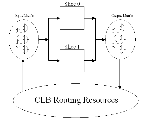
Figure 2 - CLB Overview
The primary elements in the slices are the F and G LUTs, and the X and Y flip flops. The LUTs can be used to implement gates or to implement small memories. The flip flops can be used to create state machines. The slices also have internal mux's to control the connectivity of internal resources. Finally, there is logic inside each slice to implement fast carries for arithmetic type logic.
There are 13 inputs per slice, which includes the F1-F4, G1-G4, CLK, SR, etc. Each input has a mux associated with it that determines which wire drives the input. Using JBits, each input mux has its own class with the names shown on the figure below.
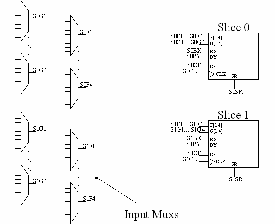
Figure 3 - Input Muxs
There are 8 output mux's, Out0 - Out7 per CLB. Each output mux can select various slice outputs and drive those signals onto the general routing. A slice output can be fanned out to multiple locations by driving multiple output muxs. Using JBits, each output mux has its own class with the names shown in the figure below.
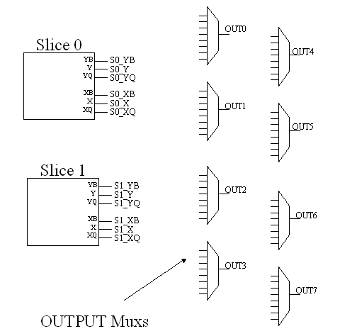
Figure 4 - Output Muxs
The general routing uses two kinds of wires: singles and hex's. Singles terminate at an adjacent CLB, while Hex's terminate at CLBs 6 positions over. Singles should be used to transport data between local CLBs, whereas Hex's should be used to transport data to non-local CLBs.
The singles and hex's are each grouped into busses that extend in the four primary directions: north, east, south, and west. The connections to neighboring CLBs are straightforward. A north single connects directly to a south single in the CLB above it. A hex west wire connects directly to a hex east wire on the 6th CLB over.
The single switch box enables the single lines to be connected together. For example, a single on the north bus can be connected to a single on the west bus or to a single on the south bus. The switch box allow the singles to round a corner or to extend the connection one CLB. The hex switch box enables the hex lines to be connected together. Using the hex switch box, a signal can traverse a hex line 6 CLBs up and then 6 CLBs to the west.
NOTE: In some limited cases, the hex lines can be read from the 3rd CLB over. So if a CLB in the 1st column drives a Hex East line, a CLB in the 4th column (same row) in addition to the the CLB in the 7th column (same row) can read it. These reads 3 CLBs over occur in the vertical and horizontal directions and are referred to as: HEX_HORIZ_M and HEX_VERT_M.
The main switch box allows the following:
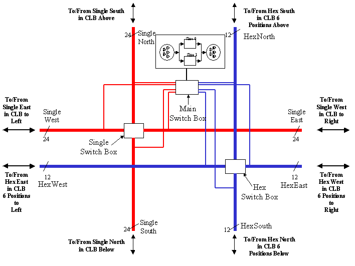
Figure 5 - CLB General Routing
Some Hex wires can only drive data into the CLB, these are uni-directional in. Some Hex wires can only drive data out of the CLB, these are unidirectional out. Some Hex wires can drive data in or out, these are bidirectional. Note however that circuit should drive data on the bidirectional lines in only one direction, not both, since this leads to contention which can damage or destroy the device.
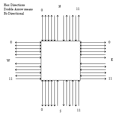
Figure 6 - Hex Directionality
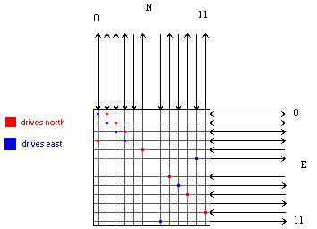
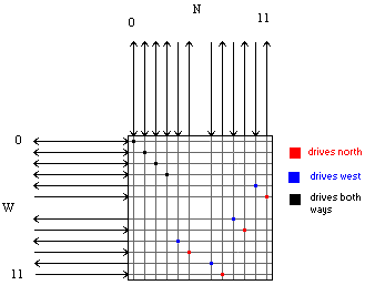
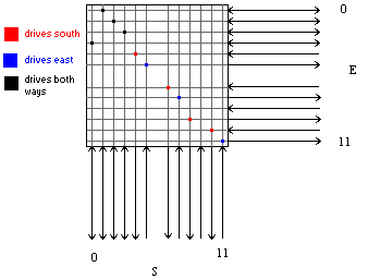
The following pictures shows the connectivity allowed by the Hex switch box.
Figure 7 - Hex North/East & North/West Connectivity
Figure 8 - Hex South/East & South/West Connectivity
Send your comments about The Virtex Architecture Guide to:
2100 Logic Drive
San Jose, CA 95124-3450
Email: JBits@xilinx.com
Last updated: 6 September 2000